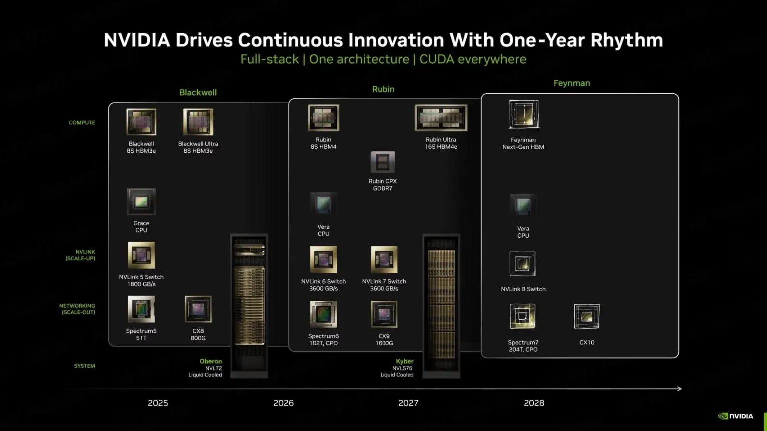
The Rubin generation hasn't even truly ramped up yet, and NVIDIA's next move is already lined up. The codename that's surfaced this time is Feynman, targeted for 2028. That may sound far off, but for the semiconductor supply chain, this kind of forward planning is itself a signal — NVIDIA has no intention of waiting until one generation is fully digested before thinking about the next.
Feynman will be built on TSMC's A16 process, which is both a process node question and a capacity-reservation question. What's even more worth noting is the shift in interface design: this will mark NVIDIA's first use of CPO (Co-Packaged Optics) technology in an AI accelerator, integrating optical interconnects directly into the chip package to take over part of the role traditionally played by copper wiring. For AI computing architectures that have long been bottlenecked by memory bandwidth and inter-chip transfer speeds, this is an issue that upcoming generations will have to confront — and NVIDIA has chosen to formally introduce it with the Feynman generation.
The information currently public is limited to the process node, the CPO technology direction, and the 2028 mass-production timeline. Specifications, supply chain division of labor, and specific product models have not yet been disclosed, and further details await confirmation from NVIDIA.